- 您现在的位置:买卖IC网 > Sheet目录334 > ISL6622AIBZ (Intersil)IC MOSFET DRVR SYNC BUCK 8-SOIC
ISL6622A
Absolute Maximum Ratings
Thermal Information
Supply Voltage (VCC, UVCC, LVCC) . . . . . . . . . . . . . . . . . . . . .15V
Thermal Resistance
θ JA (°C/W)
θ JC (°C/W)
BOOT Voltage (V BOOT-GND ). . . . . . . . . . . . . . . . . . . . . . . . . . . .36V
Input Voltage (V PWM ) . . . . . . . . . . . . . . . . . . . . . . GND - 0.3V to 7V
UGATE. . . . . . . . . . . . . . . . . . . V PHASE - 0.3V DC to V BOOT + 0.3V
V PHASE - 3.5V (<100ns Pulse Width, 2μJ) to V BOOT + 0.3V
LGATE . . . . . . . . . . . . . . . . . . . . . . .GND - 0.3V DC to V LVCC + 0.3V
GND - 5V (<100ns Pulse Width, 2μJ) to V LVCC + 0.3V
PHASE. . . . . . . . . . . . . . . . . . . . . . . . . . . . GND - 0.3V DC to 15V DC
GND - 8V (<400ns, 20μJ) to 30V (<200ns, V BOOT-GND < 36V)
SOIC Package (Note 1) . . . . . . . . . . . . 100 N/A
DFN Package (Notes 2, 3) . . . . . . . . . . 48 7
Maximum Storage Temperature Range . . . . . . . . . .-65°C to +150°C
Pb-free reflow profile . . . . . . . . . . . . . . . . . . . . . . . . . .see link below
http://www.intersil.com/pbfree/Pb-FreeReflow.asp
Recommended Operating Conditions
Ambient Temperature Range
ISL6622AIBZ, ISL6622AIRZ . . . . . . . . . . . . . . . . .-40°C to +85°C
ISL6622ACBZ, ISL6622ACRZ . . . . . . . . . . . . . . . . . 0°C to +70°C
Maximum Operating Junction Temperature. . . . . . . . . . . . . +125°C
Supply Voltage, VCC . . . . . . . . . . . . . . . . . . . . . . . . . . 6.8V to 13.2V
Supply Voltage Range, UVCC . . . . . . . . . . . . . . . . . 4.75V to 13.2V
Supply Voltage Range, LVCC . . . . . . . . . . . . . . . . . . 4.75V to 13.2V
CAUTION: Do not operate at or near the maximum ratings listed for extended periods of time. Exposure to such conditions may adversely impact product reliability and
result in failures not covered by warranty.
NOTES:
1. θ JA is measured with the component mounted on a high effective thermal conductivity test board in free air. See Tech Brief TB379 for details.
2. θ JA is measured in free air with the component mounted on a high effective thermal conductivity test board with “direct attach” features. See
Tech Brief TB379.
3. For θ JC , the “case temp” location is the center of the exposed metal pad on the package underside.
4. Limits should be considered typical and are not production tested.
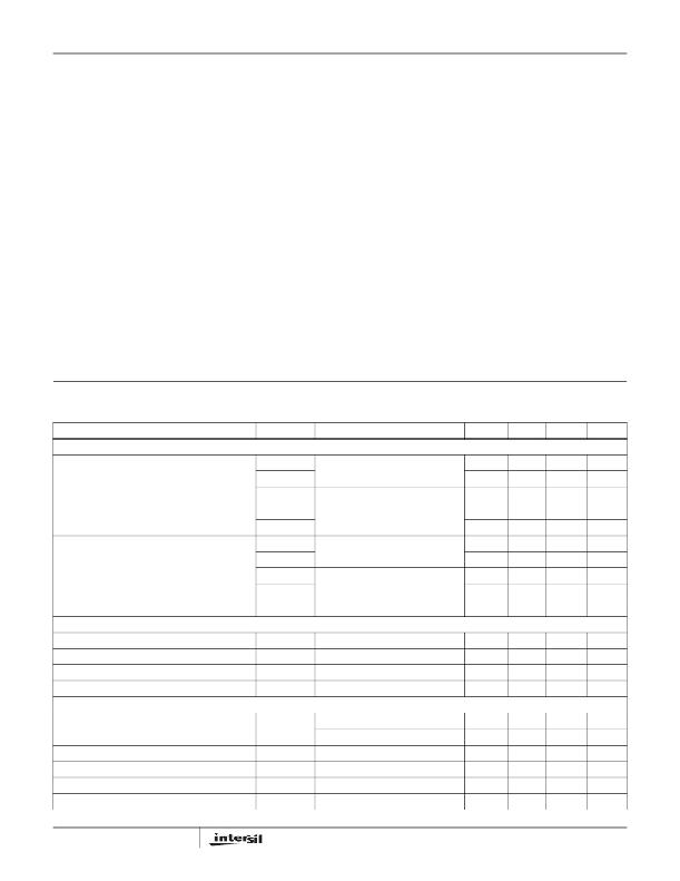
Electrical Specifications
Recommended Operating Conditions. Parameters with MIN and/or MAX limits are 100% tested at +25°C,
unless otherwise specified. Temperature limits established by characterization and are not
production tested.
PARAMETER
SYMBOL
TEST CONDITIONS
MIN
TYP
MAX
UNITS
VCC SUPPLY CURRENT (Note 4)
No Load Switching Supply Current
Standby Supply Current
I VCC
I LVCC
I VCC
I LVCC
I UVCC
I VCC
I LVCC
I VCC
I LVCC
I UVCC
ISL6622ACBZ and ISL6622AIBZ,
f PWM = 300kHz, V VCC = 12V
ISL6622ACRZ and ISL6622AIRZ,
f PWM = 300kHz, V VCC = 12V
ISL6622ACBZ and ISL6622AIBZ,
PWM Transition from 0V to 2.5V
ISL6622ACRZ and ISL6622AIRZ,
PWM Transition from 0V to 2.5V
-
-
-
-
-
-
-
-
-
-
7
3.5
4
3.5
3
5.5
0.15
5
0.15
0.5
-
-
-
-
-
-
-
-
-
-
mA
mA
mA
mA
mA
mA
mA
mA
mA
mA
POWER-ON RESET
VCC Rising Threshold
VCC Falling Threshold
LVCC Rising Threshold
LVCC Falling Threshold
6.25
4.8
4.25
3.3
6.45
5.0
4.4
3.4
6.70
5.25
4.55
3.55
V
V
V
V
PWM INPUT (See “TIMING DIAGRAM” on page 6)
Input Current (Note 4)
PWM Rising Threshold (Note 4)
PWM Falling Threshold (Note 4)
Three-State Lower Gate Falling Threshold (Note 4)
Three-State Lower Gate Rising Threshold (Note 4)
I PWM
V PWM = 5V
V PWM = 0V
VCC = 12V
VCC = 12V
VCC = 12V
VCC = 12V
-
-
-
-
-
-
500
-430
3.4
1.6
1.6
1.1
-
-
-
-
-
-
μA
μA
V
V
V
V
4
FN6601.2
March 19, 2009
发布紧急采购,3分钟左右您将得到回复。
相关PDF资料
ISL6622CBZ-T
IC MOSFET DVR SYNC BUCK 8-SOIC
ISL6801ABT
IC DRIVER HISIDE BOOTSTRAP 8SOIC
ISL78100ARZ
IC LED DRIVER AUTOMOTIVE 20-QFN
ISL8013AEVAL2Z
EVAL BOARD 2 FOR ISL8013A
ISL8014AEVAL2Z
EVAL BOARD 2 FOR ISL8014A
ISL8022EVAL2Z
EVAL BOARD 2 FOR ISL8023
ISL8088EVAL2Z
EVAL BAORD FOR ISL8088
ISL8105BEVAL2Z
EVALUATION BOARD FOR ISL8105B
相关代理商/技术参数
ISL6622AIBZ-T
功能描述:IC MOSFET DRVR SYNC BUCK 8-SOIC RoHS:是 类别:集成电路 (IC) >> PMIC - MOSFET,电桥驱动器 - 外部开关 系列:- 标准包装:50 系列:- 配置:高端 输入类型:非反相 延迟时间:200ns 电流 - 峰:250mA 配置数:1 输出数:1 高端电压 - 最大(自引导启动):600V 电源电压:12 V ~ 20 V 工作温度:-40°C ~ 125°C 安装类型:通孔 封装/外壳:8-DIP(0.300",7.62mm) 供应商设备封装:8-DIP 包装:管件 其它名称:*IR2127
ISL6622AIRZ
功能描述:IC MOSFET DRVR SYNC BUCK 10-DFN RoHS:是 类别:集成电路 (IC) >> PMIC - MOSFET,电桥驱动器 - 外部开关 系列:- 标准包装:6,000 系列:*
ISL6622AIRZ-T
功能描述:IC MOSFET DRVR SYNC BUCK 10-DFN RoHS:是 类别:集成电路 (IC) >> PMIC - MOSFET,电桥驱动器 - 外部开关 系列:- 标准包装:6,000 系列:*
ISL6622BCBZ
制造商:Intersil Corporation 功能描述:PB-FREE SYNCH BUCK MOSFET HV DRIVER, NO LDO, VR11.1, 8LD SOI - Rail/Tube 制造商:Intersil Corporation 功能描述:Gate Drivers SYNCH BUCK MSFT HV DRVR NOLDO VR11 1
ISL6622BCBZ-T
制造商:Intersil Corporation 功能描述:PB-FREE SYNCH BUCK MOSFET HV DRIVER, NO LDO, VR11.1, 8LD SOI - Tape and Reel 制造商:Intersil Corporation 功能描述:Gate Drivers SYNCH BUCK MSFT HV DRVR NOLDO VR11 1
ISL6622BCRZ
制造商:Intersil Corporation 功能描述:PB-FREE SYNCH BUCK MOSFET HV DRIVER, NO LDO, VR11.1, 10LD 3X - Rail/Tube 制造商:Intersil Corporation 功能描述:Gate Drivers SYNCH BUCK MSFT HV DRVR NOLDO VR11 1
ISL6622BCRZ-T
制造商:Intersil Corporation 功能描述:PB-FREE SYNCH BUCK MOSFET HV DRIVER, NO LDO, VR11.1, 10LD 3X - Tape and Reel 制造商:Intersil Corporation 功能描述:Gate Drivers SYNCH BUCK MSFT HV DRVR NOLDO VR11 1
ISL6622BIBZ
制造商:Intersil Corporation 功能描述:PB-FREE SYNCH BUCK MOSFET HV DRIVER, NO LDO, VR11.1, IND, 8L - Rail/Tube 制造商:Intersil Corporation 功能描述:Gate Drivers SYNCH BUCK MSFT HV DRVR NOLDO VR11 1
